CCD and CID solid-state detectors - Agilent Can Be Fun For Everyone


Getting The CCD detector at UCSF? See all 1 options To Work

Eviction oxide, i. e. the capacitor dielectric, is grown on top of the epitaxial layer and substrate. Later in the process, polysilicon gates are deposited by chemical vapor deposition, patterned with photolithography, and engraved in such a method that the separately phased gates lie perpendicular to the channels. The channels are further defined by utilization of the LOCOS process to produce the channel stop area.

Titan CCD Detector from Agilent Technologies - Labcompare.com
These channel stops are produced prior to the polysilicon gates are, as the LOCOS process makes use of a high-temperature action that would ruin eviction product. The channel stops are parallel to, and unique of, the channel, or "charge carrying", areas. Channel stops typically have a p+ drugged area underlying them, supplying a more barrier to the electrons in the charge packets (this discussion of the physics of CCD gadgets assumes an electron transfer device, though hole transfer is possible).
This will cause the CCD to deplete, near the pn junction and will gather and move the charge packages beneath the gatesand within the channelsof the device. CCD production and operation can be optimized for various uses. The above process describes a frame transfer CCD. While This Is Noteworthy might be made on a greatly drugged p++ wafer it is likewise possible to manufacture a device inside p-wells that have actually been placed on an n-wafer.
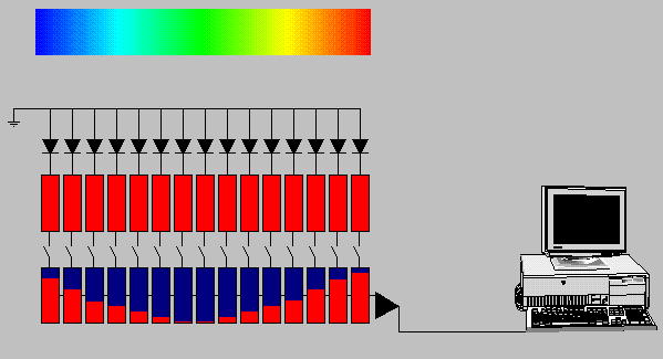
CCD sensors
What Does CCD detectors - Astrosurf Do?
This technique of manufacture is utilized in the building and construction of interline-transfer devices. Another version of CCD is called a peristaltic CCD. In a peristaltic charge-coupled gadget, the charge-packet transfer operation is analogous to the peristaltic contraction and dilation of the digestion system. The peristaltic CCD has an additional implant that keeps the charge away from the silicon/silicon dioxide user interface and generates a large lateral electric field from one gate to the next. Architecture [
modify] The CCD image sensing units can be executed in several different architectures. The most typical are full-frame, frame-transfer, and interline. The distinguishing attribute of each of these architectures is their technique to the problem of shuttering. In a full-frame device, all of the image location is active, and there is no electronic shutter. The drawback to the frame-transfer.